PCB Manufacturing
Up until now I have been making my PCBs at home (which you can read about in my previous posts), with varying levels of success. The issues mainly arose due to my heavy use of tiny surface-mount devices (SMDs), and obsession with using the smallest board possible for a design. Whenever I'm laying out a SMD board, I can't help but think that doing so requires the designer to be at least somewhat obsessive/compulsive due to the high level of concentration required for extended periods of time. If you can shut out the rest of the world and get lost in the process, it's easy.
Anyway, I can't see myself going away from the tiny-SMDs, tiny-PCBs mentality as anything else feels like I've let myself down whether due to being a waste of material/space/effort or for whatever other reason. This leaves me with two issues that have been causing me a lot of grief in my projects - transferring a design with 0.2mm (slightly less than 8mils, or 8/1000") traces and trace spacing onto PCBs, and soldering components with equally tiny pins/pads without any soldermask on the PCBs. The first issue hasn't been all that bad to deal with as it just takes more time and effort to get a good transfer, but the second issue has caused far too many boards to be scrapped. The worst part is that they get scrapped after I've already invested hours in them through the artwork transfer, etching, drilling, inserting vias, and soldering components.
That brings me to the subject of this post - I've finally decided to give a commercial PCB manufacturer a go with my latest (and greatest, of course) board. I don't want to give anything away of the designs purpose yet, so I'll just discuss its components in a non-specific way for now.
- The board consists of:
- 44 pad QFN (7x7mm)
- 36 pad QFN (10x10mm)
- 28 pad QFN (8x8mm)
- 28 pad QFN (5x5mm)
- 8 other smaller SMD ICs (most with no leads)
- Around 40-45 0402 capacitors
- Around 30 0402 resistors
- Around 10 0603 and 0805 capacitors
- A few dozen miscellaneous SMDs like ICs, connectors, etc
- The PCB is 85x60mm, double sided
For a nice picture of the sizes of some of these components, check out Curious Inventors guide to
Surface Mount Soldering. That little speck near the tip of his little finger is an 0402 component - and I have 70-80 of those to solder!
I decided to do a bit of shopping around as this was going to be my first attempt at having a PCB commercially manufactured - not so much to find the best price, but to find one that I had a way to verify that my design was acceptable and not be rejected in a few days time. This lead me to try two services,
Advanced Circuits thanks to their
Free DFM site, and
BatchPCB (SparkFun Electronics) also thanks to their DFM bot.
Advanced Circuits
I was quite impressed by the quality of Advanced Circuits FreeDFM.com service since it handled my board in my first go at running it through the verifier, and the errors (on my PCB) it provided me with were understandable and gave me everything I needed to fix them. I'm not sure if I did something wrong, but I just couldn't seem to get a good price from FreeDFMs automatic quote for my design unfortunately, so I was scared off by the prospect of paying a couple hundred dollars for a few boards of a design that I have no way of knowing would work. I'll look at them again should I need to produce at least 10 boards, but it'll simply not be worth it otherwise.
BatchPCB
BatchPCBs verifier script is unfortunately more crude than Advanced Circuits, and many times it returned PHP errors while trying to just upload my design. Once that was taken care of, I was confronted with a lovely error of "aperture 36 too small: 0.0056" (or similar). Now seriously, what are they thinking? You don't know what aperture 36 is - it's something the PCB program makes up for submitting the files to the PCB manufacturer. The only way you can know what it's talking about is to manually open the files, find a line similar to "%ADD36C,0.0056*%", change the size to something huge so it's recognisable on the board, view it in a program like ViewMate, and narrow down the problem from there. This particular error turned out to be due to a library part I was using being designed with rounded SMD pads (rather than the standard square pads) - modifying the library to use square pads fixed the problem right up.
After that was out of the way, BatchPCB did provide me with an additional error that FreeDFM did not tell me about, but I think that may have been due to FreeDFM having slightly less restrictive requirements for board layout. The final price from BatchPCB? $20 per board + $16 shipping (I ordered 3 boards, so I have a few spare just in case).
So there we go, it did take nearly a day of fiddling and Googling, but I have my first PCB order under way. As BatchPCB works as an aggregator for a Chinese PCB manufacturer, I'm not expecting to see the boards for another month due to shipping times - but maybe I'll get a pleasant surprise.
Labels: dfm, electronics, pcb
First homemade toner-transfer PCB
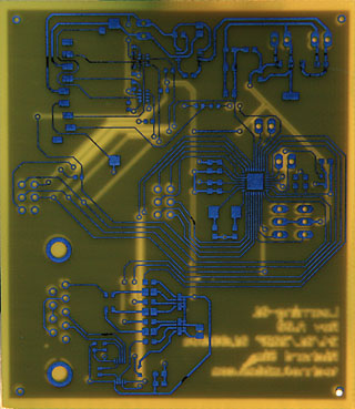
A coworker has been raving for a few weeks about how easy and quick it is to make PCBs (printed circuit boards) at home using what is commonly called the "toner transfer" method. Given that the only other way I've used to make PCBs at home (using photo-resist coated boards and a UV exposure box) had pretty terrible results and that I wasn't too eager to drop money on an untested circuit design to get it commercially made for me, it seemed worth the effort to have a go for myself.
Tom Gootee describes the method in incredible detail (if a little disorganized) on his website,
Easy PCB Fabrication. I also bought a laser printer for this purpose (well, I wanted a laser printer, and this was a good excuse...) - I decided to go for a Brother HL-5250DN as it has 1200x1200 DPI resolution as I didn't feel that a 600x600 DPI printer would be able to reproduce the SMD pads and fine traces that I would be using (0.2mm! That's less than 8mils for those of the non-metric persuasion, or about 4 'dots' at 600 DPI). I didn't diverge very far from Tom's instructions as this was my first attempt (ok, second - the first failed to transfer the toner completely to the PCB) with the exception of spending quite a bit more time ironing the design to make sure that the toner transfered this time.
I also picked up an etching kit, heater, and supplies from a local electronics store. Originally I was a bit annoyed when I opened the box to find a regular Tupperware container, an aquarium pump, and a piece of plastic to (poorly) hold the PCB while it etches - however I probably couldn't have picked up the items individually for too much cheaper anyway, so it wasn't so bad. I was hoping that the kit would contain a nice tank with graduations marked for the volume of etchant or at least depth though. Instead, the 'tank' was quite large - far larger in fact than I'll ever need - which also means that it requires a lot of etchant to fill it enough to cover even a small PCB. As I did not know this at the time, I picked up only a single 500ml bottle of Ferric Chloride (a common etchant) and as a result had to dilute it 1 part FC to 3 parts water in order to get it to just over the height of my PCB.
At this point I was having serious doubts that I'd see any success as I hadn't seen anything in any of the PCB making tutorials online about diluting FC. As it turns out, there was no problem other than it taking longer to etch, about 20 minutes I believe (but I wasn't looking at the clock). I'm sure that the heater and pump helped greatly with this, and without them I probably wouldn't have seen any results for a much longer period.
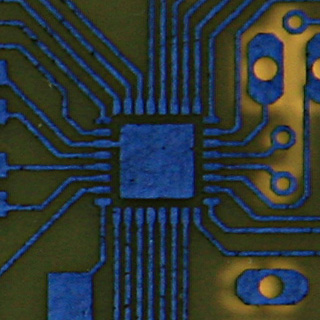
So what were the results like for my crazy-tiny traces and SMD pads? Outstanding! Considering 0.2mm is the minimum size for many commercial PCB manufacturers, and even below the minimum for some, I'm very surprised by how well even the tightest areas of the PCB turned out. To the left you can see a closeup of a MLF32 footprint IC with 0.2mm traces and spaces.
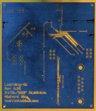
The bottom layer of the PCB has a few quite large holes in it, but I think that was mainly due to the fact that I didn't spend much time ironing that side during the toner-transfer step as it didn't have many fine traces on it. The holes didn't break any traces, so that's fine.
Labels: electronics, homemade, pcb, printed circuit board, smd, surface mount, toner, toner-transfer
V7 Navigation 1000 Menu-button bug fix
Those who have a V7 Navigation 1000 have probably noticed that the Menu (M) button doesn't actually go to the menu. It doesn't do much of anything actually (other than behave as "up" for a few menus), which is quite disappointing since there are only really 3 buttons you can use on the front (excluding the backlight on/off button) and the other two you will usually want to keep at their default functionality (zooming in and out).
Oh hey, what do you know - if you followed the instructions in my last blog entry, you will have access to change this!
- Plug the V7 Navigation 1000 into a USB port on your computer and turn it on.
- Browse to \Flash Disk\MyGuide\ in Explorer (on the PC, not the GPS).
- Copy the 1.3mb Data.zip to your PC's hard drive.
- Rename the Data.zip on the GPS to Data.orig (as a backup).
- Open the Data.zip that you copied to your PC and extract config\keybind.txt from the archive.
- Open keybind.txt in Notepad and scroll down to the [CARPOINTA1000] section.
- Below this, add the following line: UP="ROUTEINFO". The section will now look like this:
[CARPOINTA1000]
UP="ROUTEINFO"
39="ZOOMIN_DISCRETE"
37="ZOOMOUT_DISCRETE"
- Save keybind.txt and replace the original keybind.txt in Data.zip with your edited keybind.txt. Make sure that you actually replace the file and that it goes into the correct directory of Data.zip.
- Copy the updated Data.zip back to the GPS (put it back in \Flash Disk\MyGuide\).
Done and done! You can now start MyGuide and the Menu (M) button will now behave just like going to Route > Info.
You can actually replace
ROUTEINFO with many other useful commands, of which
MAINMENU is a good choice (as it is obviously the intended behavior of the Menu button, but I found
ROUTEINFO to be more useful personally). Have a look through
keybind.txt to get an idea of what other commands you can try.
Of course, if you don't use the zoom in/out buttons, you can change the bindings on those too.
Labels: bug fix, bugs, electronics, GPS, hacking, hardware, iGo, MioMap, MyGuide, PNA, software, V7
Hacking the V7 Navigation 1000 GPS
On Boxing Day I picked up a cool new toy - a V7 Navigation 1000. It's an in-car GPS unit with quite nice hardware and software (albeit perhaps matched up and configured by monkeys, and somewhat buggy too). As with any new electronics gadget, I set out looking for updates as soon as I had my hands on it - which lead me down the road of hacks for similar GPS units. It turns out that the software the V7 unit runs,
MyGuide, is just
iGo re-branded and is exactly the same as what many other common GPS units run under various names such as
MioMap.
While it's great that the Navigation 1000 has all its maps on an included 1gb SD card, this lead to the problem that they did not include any way to access the rest of the files on the device (such as the configuration files for MyGuide). Devices like the Mio DigiWalker C310S have a USB port since their maps are stored on internal Flash memory and not an SD card, and this let their owners do some simple software hacks to get full access to reconfigure the GPS software as well as directly use Windows CE. Yes, these babies run on Windows CE!
Knowing that there was Windows CE under the hood, and that there was a quite powerful processor powering the device (400MHz ARM), this lead me to assume that there must be a USB port hidden somewhere inside - perhaps behind what looked like covered up ports? After all, if I was developing a Windows CE device, I'd want a USB port for development and debugging!
And so it began...
As with all hardware hacks, please do not attempt this unless you are experienced in electronics and soldering, and have all the necessary equipment. You'll want a good soldering iron with a very fine tip (made for SMD work, not through-hole!) - not the kind you get at RadioShack.
First, start by taking off the front case. There are 4 small phillips screws on the back of the V7 Navigation 1000 that you'll have to remove. None of my phillips jewelers screwdrivers were small enough to fit into the screw hole, so I used one of my medium-sized flat-head jewelers screwdrivers - it worked fine. As with most gadgets, the case is also sealed by plastic clips around the edge. After several attempts with my trusty jewelers screwdriver that had just saved me, I gave up and used my thumb nail. In no time I had the case open. Woohoo!
With the case open, the first thing you'll see is most of the PCB is covered in shielding tape (which is very sticky!). I'll tell you now - all the interesting components are inside a metal shield on the back of the PCB, and it's soldered down pretty damn well. After I came to that realization, I almost packed in the towel as I assumed that any way to access USB would also be hidden in there. While I did some last minute poking around the PCB, I saw 4 test points marked J3. Test points marked as a jumper? Very odd... and being that USB uses 4 wires (+, -, D+, D-), I had a "eureka!" moment.
Where will you find these golden test points (no, seriously - they are gold plated)? At the very top of the front of the PCB, nearly in the centre (above a whole lot of VIAs as it would seem that the ARM chip is in a BGA package). To get to them you will have to remove the shielding tape from the top of the PCB - it's easy enough as it's only stuck to the top of a few components, so just take it slow and be careful.
If you look closely at J3, you will see that of the 4 test points, the left-most test point is separated from the other 3. This is VCC (V+). Looking closely at the right-most test point, you can see that it is connected to the ground plane. This is GND (V-). As for the other 2, I had no idea other than the standard order is V+, D-, D+. GND. As V+ and GND were in the correct order, I went with the assumption that D- and D+ were too. I was right. At least some people follow standards! :)
We now have a way to connect to this device by USB, all we need now is to connect it up. I had the choice of soldering a USB cable directly to the PCB or putting a mini-USB connector in the unit and being able to plug a standard mini-USB cable in, and would definitely have gone with the later if I wasn't in a rush to see if all my assumptions about the USB pinout was correct (or if it even was a USB port). As such, I found a spare mini-USB cable, cut off the mini-USB plug, and stripped the 4 wires. If your USB cable has shielding (it should), just cut that back also. You'll want about 10cm of the USB cables shielding stripped back, as it's too fat to route through the GPS unit. Next, strip the ends of the 4 wires in the cable. You only want to have 1-2mm (that's a bit less than 0.05-0.1") of bare wire at the ends, as the actual test points that you'll be soldering them to are about 1mm in diameter each and any extra bare wire could easily make contact with other wires or components causing all kinds of grief (and likely a dead GPS and perhaps PC too if it's connected at the time).
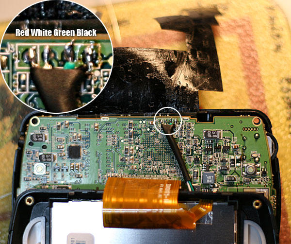
You can see that I've soldered them in the order (left-to-right) Red, White, Green, Black. These are the standard colours for VCC, D-, D+, and GND respectively in USB cables, and as such they should be the same in any USB cable that you cut up for this hack. If they are not, or if you just want to be extra careful (I was!), you can always use a continuity tester on the mini-USB connector that you cut off from the end of the cable (
pinout).
You should also note the use of heat-shrink tubing (and further on the use of electrical tape) to prevent any of the USB wires (and shielding of the USB cable itself!) coming into contact with the PCB or components where they shouldn't.
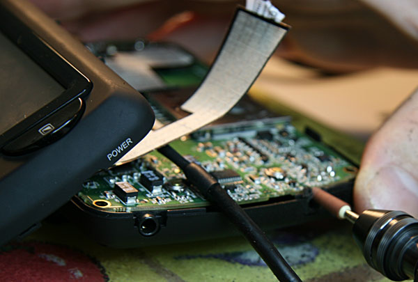
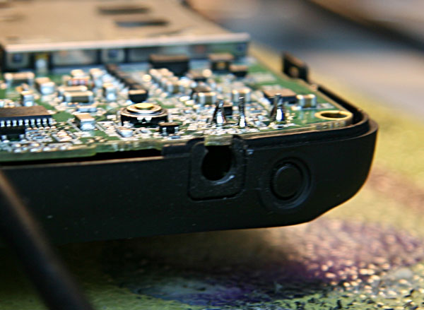
Next up we need to make a hole to feed the USB cable out from. I chose to make use of the area above the power button as it looked like it was originally designed to have a port there (the PCB even had room for an unknown connector - but it wasn't USB). You can make it anywhere on the case obviously, another good location would be the top next to the stylus as that would minimize the internal-routing of the USB cable (given the amount of shielding the GPS unit has, this would likely be a good thing). Dremel time!
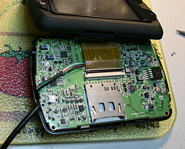
When routing the USB wires, be careful to avoid blocking the front-panel buttons and their backlight LEDs. I found it was quicker to just turn the unit on than to look around the PCB for the 4 LEDs. When that's done, you should have something looking like this.
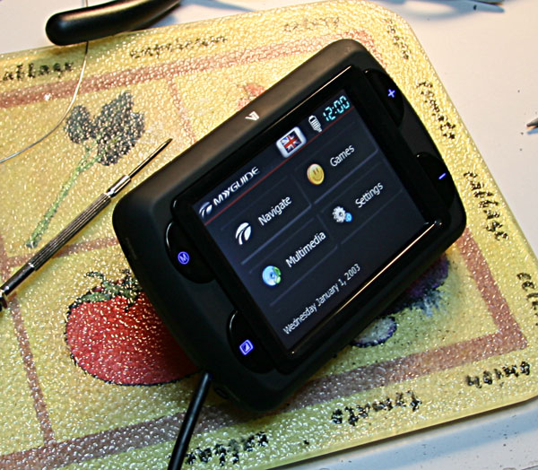
Snap the case back on and put the 4 screws back in, and you're done! You might want to turn it on now to make sure that it still works...
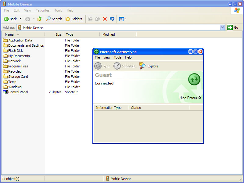
Download and install Microsoft ActiveSync (
here) as this will let you access the device just like it was a PDA. Plug the GPS unit into one of your computer's USB ports, and you should be good to go! If you click 'Explore' in ActiveSync, Explorer will open to allow you to browse around the file system. The first thing you should do is back everything up, though there are some files that you cannot (system files).
One easy hack you can make right off the bat with MyGuide is to add a button from the startup screen to run Explorer on your device. To do this, copy
\Flash Disk\IGOPATH.TXT to your PC and create a backup copy of it also. Rename the file on the device to
IGOPATH.bak. Back on your PC, open
IGOPATH.TXT in Notepad and add the following line to the end of the
[Multimedia] section (so this should be the last line in the file):
Explorer= "icons/files.bmp", "\\Windows\\Explorer.exe"
The file should now look like this:
[pre_init]
LangSyncOn = "\\flash disk\\langsync.exe"
[pre_quit]
LangSyncOff = "\\flash disk\\langsync.exe"
[modules]
Settings = "icons/settings.bmp", "settings", 1
Multimedia = "icons/media.bmp", "Multimedia", 0
[Multimedia]
Picture= "", "\\Flash DIsk\\XImage\\XImage.exe"
Movie= "", "\\Flash DIsk\\XMovie\\XMovie.exe"
Music= "", "\\Flash DIsk\\XMp3\\XMp3.exe"
Explorer= "icons/files.bmp", "\\Windows\\Explorer.exe"
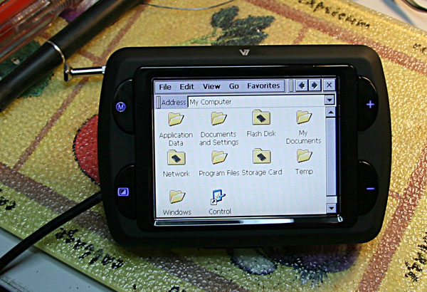
You can now copy this file back to the V7 Navigation 1000 (under
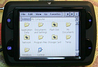
\Flash Disk\, of course), then power-cycle the device so it gets the new configuration. If you click on Multimedia on the first screen now, it will list Music, Movie, Picture, and... Explorer! Tap on Explorer, and there you have it - Windows CE Explorer is running on your V7 Navigation 1000.
From here you can go ahead and install lots of normal Windows CE software such as games, and utilities, or just mess around with MyGuides configuration (custom skins, hidden features, and more are all possible... maybe even bug fixes). Since the Mio uses the same software, a lot of its hacks should be portable to the V7.
The
GpsPasSion forums are a great source of information on Mio hacking, so should be one of your first stops.
Happy hacking, and if you find something cool, drop me a note!
Labels: electronics, GPS, hacking, hardware, iGo, MioMap, MyGuide, PNA, V7


 Atom
Atom
