First homemade toner-transfer PCB
 A coworker has been raving for a few weeks about how easy and quick it is to make PCBs (printed circuit boards) at home using what is commonly called the "toner transfer" method. Given that the only other way I've used to make PCBs at home (using photo-resist coated boards and a UV exposure box) had pretty terrible results and that I wasn't too eager to drop money on an untested circuit design to get it commercially made for me, it seemed worth the effort to have a go for myself.
Tom Gootee describes the method in incredible detail (if a little disorganized) on his website, Easy PCB Fabrication. I also bought a laser printer for this purpose (well, I wanted a laser printer, and this was a good excuse...) - I decided to go for a Brother HL-5250DN as it has 1200x1200 DPI resolution as I didn't feel that a 600x600 DPI printer would be able to reproduce the SMD pads and fine traces that I would be using (0.2mm! That's less than 8mils for those of the non-metric persuasion, or about 4 'dots' at 600 DPI). I didn't diverge very far from Tom's instructions as this was my first attempt (ok, second - the first failed to transfer the toner completely to the PCB) with the exception of spending quite a bit more time ironing the design to make sure that the toner transfered this time.
 I also picked up an etching kit, heater, and supplies from a local electronics store. Originally I was a bit annoyed when I opened the box to find a regular Tupperware container, an aquarium pump, and a piece of plastic to (poorly) hold the PCB while it etches - however I probably couldn't have picked up the items individually for too much cheaper anyway, so it wasn't so bad. I was hoping that the kit would contain a nice tank with graduations marked for the volume of etchant or at least depth though. Instead, the 'tank' was quite large - far larger in fact than I'll ever need - which also means that it requires a lot of etchant to fill it enough to cover even a small PCB. As I did not know this at the time, I picked up only a single 500ml bottle of Ferric Chloride (a common etchant) and as a result had to dilute it 1 part FC to 3 parts water in order to get it to just over the height of my PCB.
At this point I was having serious doubts that I'd see any success as I hadn't seen anything in any of the PCB making tutorials online about diluting FC. As it turns out, there was no problem other than it taking longer to etch, about 20 minutes I believe (but I wasn't looking at the clock). I'm sure that the heater and pump helped greatly with this, and without them I probably wouldn't have seen any results for a much longer period.
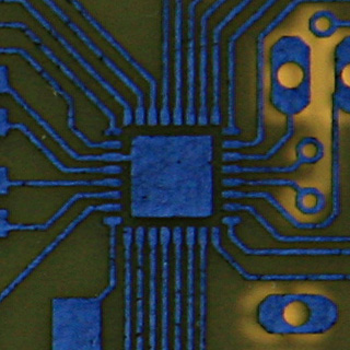 So what were the results like for my crazy-tiny traces and SMD pads? Outstanding! Considering 0.2mm is the minimum size for many commercial PCB manufacturers, and even below the minimum for some, I'm very surprised by how well even the tightest areas of the PCB turned out. To the left you can see a closeup of a MLF32 footprint IC with 0.2mm traces and spaces.
The bottom layer of the PCB has a few quite large holes in it, but I think that was mainly due to the fact that I didn't spend much time ironing that side during the toner-transfer step as it didn't have many fine traces on it. The holes didn't break any traces, so that's fine.
Labels: electronics, homemade, pcb, printed circuit board, smd, surface mount, toner, toner-transfer
posted by Richard Sim @ 1/26/2007 12:30:00 AM
![]()


0 Comments:
Post a Comment
<< Home